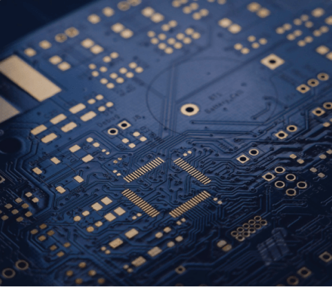
Custom IC Layout Design
NokshaSemi's IC layout design team brings extensive technology and EDA expertise, honed over years of working with process nodes from 180nm to the latest technologies. We excel in both analog and digital layout design, providing high-quality layouts that are optimized for performance and area

Our Expertise Include
- Standard Library Cells: Expertly crafted for optimal performance, area, and power efficiency.
- Memory Cells: Specialized in high-density and low-power SRAM, DRAM, and TCAM designs.
- I/O Circuits: Custom-designed for robust interfacing with external components.
- ADC And DAC: Precision layouts for high-resolution and low-noise analog-to-digital and digital-to-analog converters.
- Band Gap Reference(BGR): Stable and accurate voltage reference circuits for various applications.
- Analog And Digital Layout Design: Comprehensive solutions for mixed-signal designs, ensuring seamless integration.
- Power Management Units: Efficient power distribution and regulation circuits for low power consumption.
- Low Power Custom Circuit Design: Tailored designs to minimize power usage without sacrificing performance.
- Custom SRAM/DRAM/TCAM Design: High-speed and low-leakage memory layouts for advanced applications.
- PLLs, DLLs & Oscillators: Precision timing circuits for clock generation and synchronization.
Our dedicated R&D team continually advances our architecture and design methods, ensuring we remain at the forefront of the fast-paced IC industry. Whether you need cutting-edge analog circuit designs or reliable post-silicon validation, Noksha Semi has the expertise and technology to deliver exceptional results.